Communication-concepts MJE243 Manuel d'utilisateur

Naviguer en ligne ou télécharger Manuel d'utilisateur pour Matériel Communication-concepts MJE243. Communication Concepts MJE243 User Manual Manuel d'utilisatio

  • Télécharger
  • Ajouter à mon manuel
  • Imprimer
  • Page
    / 6
  • Table des matières
  • MARQUE LIVRES
  • Noté. / 5. Basé sur avis des utilisateurs
Vue de la page 0
© Semiconductor Components Industries, LLC, 2009
April, 2009 Rev. 13
1 Publication Order Number:
MJE243/D
MJE243 - NPN,
MJE253 - PNP
Complementary Silicon
Power Plastic Transistors
These devices are designed for low power audio amplifier and
lowcurrent, highspeed switching applications.
Features
High CollectorEmitter Sustaining Voltage
V
CEO(sus)
= 100 Vdc (Min)
High DC Current Gain @ I
C
= 200 mAdc
h
FE
= 40200
= 40120
Low CollectorEmitter Saturation Voltage
V
CE(sat)
= 0.3 Vdc (Max) @ I
C
= 500 mAdc
High Current Gain Bandwidth Product
f
T
= 40 MHz (Min) @ I
C
= 100 mAdc
Annular Construction for Low Leakages
I
CBO
= 100 nAdc (Max) @ Rated V
CB
PbFree Packages are Available*
MAXIMUM RATINGS
Rating Symbol Value Unit
CollectorEmitter Voltage V
CEO
100 Vdc
CollectorBase Voltage V
CB
100 Vdc
EmitterBase Voltage V
EB
7.0 Vdc
Collector Current Continuous
Peak
I
C
4.0
8.0
Adc
Base Current I
B
10 Adc
Total Power Dissipation @ T
C
= 25_C
Derate above 25_C
P
D
15
120
W
mW/_C
Total Power Dissipation @ T
A
= 25_C
Derate above 25_C
P
D
1.5
12
W
mW/_C
Operating and Storage Junction
Temperature Range
T
J
, T
stg
65 to +150
_C
THERMAL CHARACTERISTICS
Characteristic Symbol Max Unit
Thermal Resistance, JunctiontoCase
q
JC
8.34
_C/W
Thermal Resistance,
JunctiontoAmbient
q
JA
83.4
_C/W
Maximum ratings are those values beyond which device damage can occur.
Maximum ratings applied to the device are individual stress limit values (not
normal operating conditions) and are not valid simultaneously. If these limits are
exceeded, device functional operation is not implied, damage may occur and
reliability may be affected.
*For additional information on our PbFree strategy and soldering details, please
download the ON Semiconductor Soldering and Mounting Techniques
Reference Manual, SOLDERRM/D.
Device Package Shipping
ORDERING INFORMATION
MJE243 TO225 500 Units/Box
4.0 AMPERES
POWER TRANSISTORS
COMPLEMENTARY SILICON
100 VOLTS, 15 WATTS
http://onsemi.com
MJE243G
TO225
(PbFree)
500 Units/Box
TO225
CASE 77
STYLE 1
2
1
3
MARKING DIAGRAM
YWW
JE2x3G
Y = Year
WW = Work Week
JE2x3 = Device Code
x = 4 or 5
G=PbFree Package
Preferred devices are recommended choices for future use
and best overall value.
MJE253 TO225 500 Units/Box
MJE253G
TO225
(PbFree)
500 Units/Box
Vue de la page 0
1 2 3 4 5 6

Résumé du contenu

Page 1 - Power Plastic Transistors

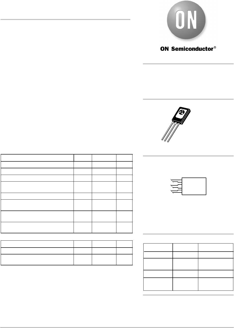
© Semiconductor Components Industries, LLC, 2009April, 2009 − Rev. 131 Publication Order Number:MJE243/DMJE243 - NPN,MJE253 - PNPComplementary Silico

Page 2 - ELECTRICAL CHARACTERISTICS (T

MJE243 − NPN, MJE253 − PNPhttp://onsemi.com2ELECTRICAL CHARACTERISTICS (TC = 25_C unless otherwise noted)CharacteristicSymbol Min Max UnitOFF

Page 3 - Figure 4. Thermal Response

MJE243 − NPN, MJE253 − PNPhttp://onsemi.com31620Figure 1. Power DeratingT, TEMPERATURE (°C)040 60 100 120 16012PD, POWER DISSIPATION (WATTS)1.

Page 4 - Figure 6. Turn−Off Time

MJE243 − NPN, MJE253 − PNPhttp://onsemi.com410VCE, COLLECTOR-EMITTER VOLTAGE (VOLTS)0.1300.010.05Figure 5. Active Region Safe Operating Area50

Page 5

MJE243 − NPN, MJE253 − PNPhttp://onsemi.com5IC, COLLECTOR CURRENT (AMP)IC, COLLECTOR CURRENT (AMP)IC, COLLECTOR CURRENT (AMP)hFE, DC CURRENT G

Page 6 - PACKAGE DIMENSIONS

MJE243 − NPN, MJE253 − PNPhttp://onsemi.com6PACKAGE DIMENSIONSTO−225CASE 77−09ISSUE ZNOTES:1. DIMENSIONING AND TOLERANCING PER ANSIY14.5M, 198

Commentaires sur ces manuels

Pas de commentaire